

Axelera AI unveils third generation of Titania AI accelerator with LPDDR6 memory
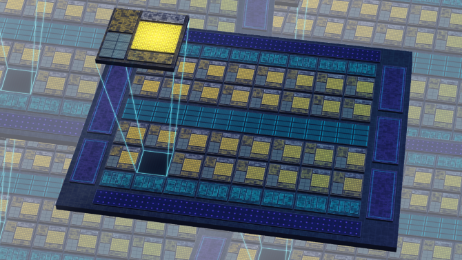
The Dutch company Axelera AI has unveiled the third generation of its Titania AI accelerator with LPDDR6 memory instead of HBM. The chip is manufactured by TSMC (4nm), with mass production planned for Q3 2027.
The Dutch company Axelera AI has unveiled the third generation of its AI inference architecture called Titania. The chip is being developed as part of the European DARE project, in which, alongside Axelera, Brno-based Codasip is working on a server processor and the Spanish company Openchip on a vector accelerator for high precision (FP64); the goal is European technology for AI data centers and supercomputers. Titania has a chiplet design — a single package combines two chiplets and offers 64 AI cores and 32 programmable RISC-V cores with vector units, with native support for FP8 (2.5 petaflops) and FP4. It will be manufactured using TSMC's 4nm process.
Instead of HBM memory, the chip uses 128 GB of LPDDR6 with a bandwidth of 2 458 GB/s and 128 MB of SRAM. According to the company, for Mixture-of-Experts type models, capacity and efficient memory utilization matter more than raw bandwidth, which reduces price, power consumption, and supply chain dependency — while also eliminating the need for expensive advanced packaging such as TSMC CoWoS. The chip can be deployed as a PCIe 6.0 card, an OCP/UBB board, or an OAM module, with power consumption of roughly 400 W.
The reference air-cooled AX8 server (4U) houses eight Titania packages, achieves 20 PFLOPS (FP8), has 1 TB of LPDDR6 memory with a bandwidth of 19.6 TB/s, and according to the manufacturer can serve a model up to 1.6 trillion parameters in size (FP4) including headroom for KV cache. The server's power consumption is 5–6 kW. The company states up to seven times better performance per watt and up to twenty times better TCO compared to competing servers, but these figures so far come only from the manufacturer's own simulations, not from independent tests.
Mass production is planned for the third quarter of 2027, with broader availability of PCIe cards and the first customer deployments planned for early 2028. The company states preliminary orders worth over $300 million.
Why it matters
For companies operating or planning AI inference infrastructure, this represents a potential European alternative to solutions built on expensive and scarce HBM memory and advanced packaging, which could reduce costs and dependency on the supply chain centered around Nvidia and TSMC CoWoS. However, the practical impact is still distant — mass production is planned only for Q3 2027 and actual deployments for early 2028, and the key performance and cost (TCO) comparisons so far come only from the manufacturer's simulations.
Relevant practical impact
What this means
For a business
Companies planning investments in AI inference infrastructure are prospectively gaining a European alternative to Nvidia solutions, according to the manufacturer with lower power consumption and significantly lower operating costs (TCO) — but actual deployment is realistic only in 2027–2028, and the key figures so far come from the manufacturer's simulations.
StrategyCheck the original
Event sources
only one source so far · 1 publisher, 1 independent. We count feeds from the same owner only once.